Newly detected
TAS5630 chip can solve my problems about the PWM amplifier. This chip have analog inputs, the package contains all required parts (A/D converter, PWM modulator), and the parallel mode is possible if less than 4 Ohm output impedance required. with this package we have one paralleled mono or one stereo poweramp with analog input.
But I have TAS5261 chips, without analog input. For this design required TAS55xx PWM modulators and analog/digital converters. These chips recommended for home DVD players, the power supply is 3.3 volts only. I don't think that this solution is ideal for instrument amplification.
In this post, I writing about the method and simulation of analog PWM modulator.
First I need a triangle function generator. I found too much... The clock of PWM input TAS chip is 192-384 kHz, what is understandable if digital chips placed before chip. For this frequency, not too easy to find triangle signal generator with very good output.
Can be found one-chip function generators. One of them is
LM566 (with this chip I found a schematic) not available here and now, or we can use
XR2206 or
ICL8038 chips. These chips are very simple solutions for triangle output, maybe I will try some of them. The maximum frequency on the datasheet is 0.5MHz, typical is 1MHz, but the 8038 have 300kHz maximum. I have no experiences with these function generator chips, so I don't know about the output quality. This is the reason, why I seek discreet analog function generator for triangle output. The another reason, is, function generator chips are not available on Multisim.
The first tryouts I have no success:
This function generator promised for perfect output, but the triangle with 20 kHz only is really bad. So I don't need to try this design for 200-300 kHz.
I tried more triangle generators with op-amps, but the output is not good enough. Finally I found a really good analog triangle generator with nice triangle and square outputs. This circuit can be used up to 4MHz what is more than enough.
I have good result on 300kHz:
See the simulation output, this is 235 kHz. Very easy to set the frequency and duty cycle.
I tested this discreet (but easy to set) schematic on higher frequency. Here ate the test results:
1.3 MHz:
2MHz:
3.5 MHz:

6 MHz:
I think, if the upper schematic is good enough on 2-4 MHz, then this is good for around 300 kHz only.
The triangle output of this circuit wired to the fast comparator. the most of comparators doesn't worked on Multisim for me, but finally I found one what is very good for output simulation:
Example about the signals in the circuit:
The purple line is the triangle output of function generator, the green is the part of 1kHz sinus (audio) input, the red is the TTL PWM modulated square with variable duty cycle.
In this image can be seen how duty cycle modulated by the sinus input signal:
Continued the circuit simulation, the next is the comparator. This
part AD8611 is good on Multisim, but I think another comparator (for
example LM311) is good on real life too. The triangle signal and the audio (sinus) input have to be connected to the comparator's inputs.
The most important question is, the quality of the PWM modulated output. What I get back, if the PWM modulated square signal converted back to the original sinus wave. The quality of this method cannot seen by the quality of the PWM modulated output. See the image:
The green line is the original audio sine wave signal. I have to get back this wave from the PWM outputs. The dark-red is the (good) result if the PWM output converted back to the original sine. What is the blue line, I will tell you soon....
After the comparator chip, I put TTL logic. This logic made soft start while the triangle generator up, and disabled the input of TAS H-bridge. This method made inverted and non-inverted PWM outputs. Finally this is the "deat time" logic. The TAS5261 contains "dead time" logic, and the most if comparators have inverted and non-inverted outputs. This TTL logic required, if the output of PWM amplifier is simple MOSFETs, not H-bridge chips with internal logic what I want to use.
......the blue line (what is really wrong and distorted) is the converted output of TTL chips.

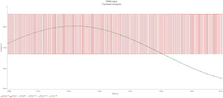
Here are the signals in this design: The sine is 20 kHz now, the blue line is the triangle signal on 235 kHz, the red line is the TTL PWM output, the tall brown line is the output of comparator. The result is much better on the comparator output.
After simulation results I have many problems.
The first question is about the precision of simulation. How about the simulation and the reality, whats about the differences, depending on the PCB design and the quality of parts.
After these PWM modulated square waves, I have to put TAS H-bridhe chips, and I can use these outputs for audio. Maybe this method have good result, but maybe not. Maybe the TTL outputs (what is really wrong after decoding on the simulation result) good enough for discreet MOSFET drivers. Finally I have to test the DC offset of comparator inputs and outputs, and the linear frequency range of the decoded output. These solutions is on the next post.


